In the absence of confirmation by device specification sheets, SHARP takes no responsibility for any defects that may occur in equipment using any SHARP devices shown in
catalogs, data books, etc. Contact SHARP in order to obtain the latest device specification sheets before using any SHARP device.
1
DESCRIPTION
The LZ23J3V is a 1/2.7-type (6.72 mm) solid-state
image sensor that consists of PN photo-diodes
and CCDs (charge-coupled devices). With
approximately 1 310 000 pixels (1 344 horizontal x
971 vertical), the sensor provides a stable high-
resolution color image.
FEATURES
∑ Optical size : 6.72 mm (aspect ratio 4 : 3)
∑ Interline scan format
∑ Square pixel
∑ Number of effective pixels : 1 292 (H) x 966 (V)
∑ Number of optical black pixels
≠ Horizontal : 3 front and 49 rear
≠ Vertical : 3 front and 2 rear
∑ Number of dummy bits
≠ Horizontal : 28
≠ Vertical : 2
∑ Pixel pitch : 4.2 µm (H) x 4.2 µm (V)
∑ R, G, and B primary color mosaic filters
∑ Supports monitoring mode
∑ Low fixed-pattern noise and lag
∑ No burn-in and no image distortion
∑ Blooming suppression structure
∑ Built-in output amplifier
∑ Built-in overflow drain voltage circuit and reset
gate voltage circuit
∑ Variable electronic shutter
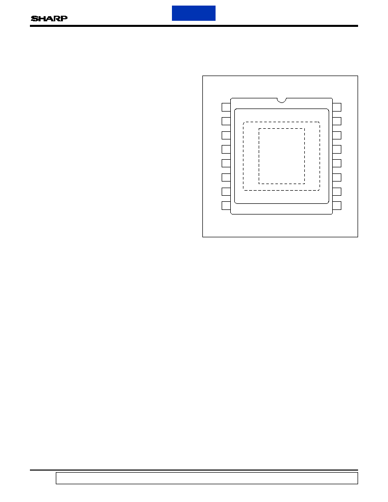
∑ Package :
16-pin shrink-pitch WDIP [Plastic]
(WDIP016-P-0500C)
Row space : 12.70 mm
PIN CONNECTIONS
PRECAUTIONS
∑ The exit pupil position of lens should be 15 to 50
mm from the top surface of the CCD.
∑ Refer to "PRECAUTIONS FOR CCD AREA
SENSORS" for details.
LZ23J3V
1/2.7-type Interline Color CCD Area
Sensor with 1 310 k Pixels
LZ23J3V
1
OD
2
GND
3
OFD
4
PW
5
ÿ
RS
6
NC
7
ÿ
H1
8
16
15
14
13
12
11
10
9
ÿ
H2
OS
GND
ÿ
V1A
ÿ
V1B
ÿ
V2
ÿ
V3A
ÿ
V3B
ÿ
V4
16-PIN SHRINK-PITCH WDIP
TOP VIEW
(WDIP016-P-0500C)
Back
2
LZ23J3V
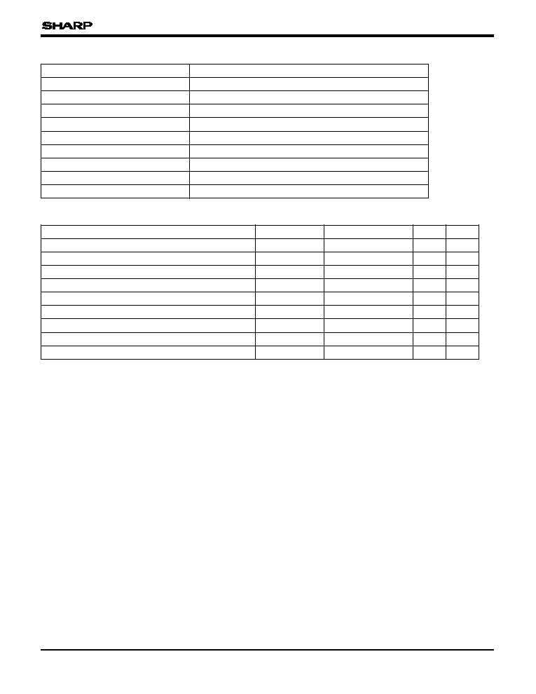
PIN DESCRIPTION
SYMBOL
PIN NAME
OD
Output transistor drain
OS
Output signals
ÿ
RS
Reset transistor clock
ÿ
V1A
, ÿ
V1B
, ÿ
V2
, ÿ
V3A
, ÿ
V3B
, ÿ
V4
Vertical shift register clock
ÿ
H1
, ÿ
H2
Horizontal shift register clock
PW
P-well
GND
Ground
NC
No connection
Overflow drain
OFD
ABSOLUTE MAXIMUM RATINGS
(T
A
= +25 ∞C)
PARAMETER
SYMBOL
RATING
UNIT
Output transistor drain voltage
V
OD
0 to +18
V
Reset gate clock voltage
V
ÿRS
Internal output
V
Vertical shift register clock voltage
V
ÿV
V
PW
to +18
V
Horizontal shift register clock voltage
V
ÿH
≠0.3 to +12
V
Voltage difference between P-well and vertical clock
V
PW
-V
ÿV
≠29 to 0
V
Storage temperature
T
STG
≠40 to +85
∞C
Ambient operating temperature
T
OPR
≠20 to +70
∞C
2
NOTE
NOTES :
1. Do not connect to DC voltage directly. When OFD is connected to GND, connect V
OD
to GND. Overflow drain clock is
applied below 33 Vp-p.
2. Do not connect to DC voltage directly. When ÿ
RS
is connected to GND, connect V
OD
to GND. Reset gate clock is
applied below 8 Vp-p.
3. When clock width is below 10 µs, and clock duty factor is below 0.1%, voltage difference between vertical clocks will be
below 28 V.
1
V
Internal output
V
OFD
Overflow drain voltage
3
V
0 to +17
V
ÿV
-V
ÿV
Voltage difference between vertical clocks
3
LZ23J3V
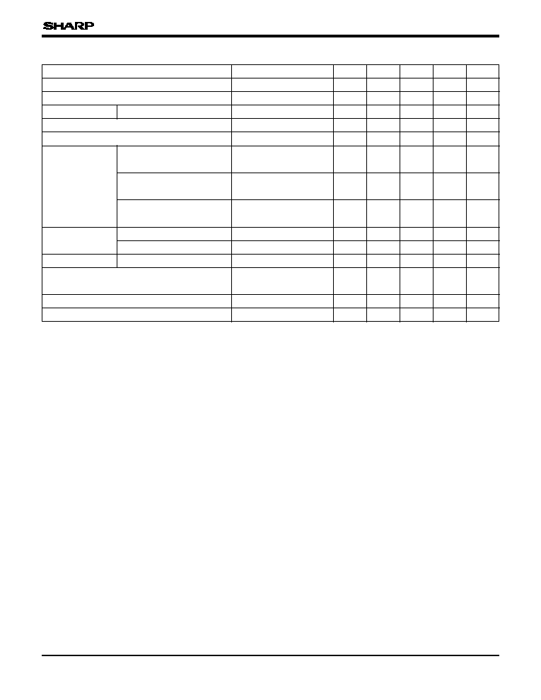
RECOMMENDED OPERATING CONDITIONS
PARAMETER
SYMBOL
MIN.
TYP.
MAX.
UNIT
NOTE
Ambient operating temperature
T
OPR
25.0
∞C
Output transistor drain voltage
V
OD
15.0
15.5
16.0
V
NOTES :
1. Use the circuit parameter indicated in "SYSTEM CONFIGURATION EXAMPLE", and do not connect to DC voltage directly.
2. V
PW
is set below V
ÿVL
that is low level of vertical shift register clock, or is used with the same power supply that is connected
to V
L
of V driver IC.
* To apply power, first connect GND and then turn on V
OD
. After turning on V
OD
, turn on PW first and then turn on other powers
and pulses. Do not connect the device to or disconnect it from the plug socket while power is being applied.
1
V
32.0
30.0
28.0
V
ÿOFD
Overflow drain clock
P-well voltage
V
PW
≠10.0
V
ÿVL
V
2
Ground
GND
0.0
V
V
≠7.5
≠8.0
≠8.5
V
ÿV1AL
, V
ÿV1BL
, V
ÿV2L
V
ÿV3AL
, V
ÿV3BL
, V
ÿV4L
Vertical shift
register clock
LOW level
INTERMEDIATE level
HIGH level
V
ÿV1AI
, V
ÿV1BI
, V
ÿV2I
V
ÿV3AI
, V
ÿV3BI
, V
ÿV4I
V
ÿV1AH
, V
ÿV1BH
V
ÿV3AH
, V
ÿV3BH
15.0
0.0
15.5
16.0
V
V
LOW level
Horizontal shift
register clock
V
ÿH1L
, V
ÿH2L
≠0.05
0.0
0.05
V
HIGH level
V
ÿH1H
, V
ÿH2H
4.5
5.0
5.5
V
1
V
5.5
5.0
4.5
V
ÿRS
Reset gate clock
p-p level
Reset gate clock frequency
f
ÿRS
12.27
MHz
Horizontal shift register clock frequency
f
ÿH1
, f
ÿH2
12.27
MHz
Vertical shift register clock frequency
f
ÿV1A
, f
ÿV1B
, f
ÿV2
f
ÿV3A
, f
ÿV3B
, f
ÿV4
7.87
kHz
p-p level
LZ23J3V
4
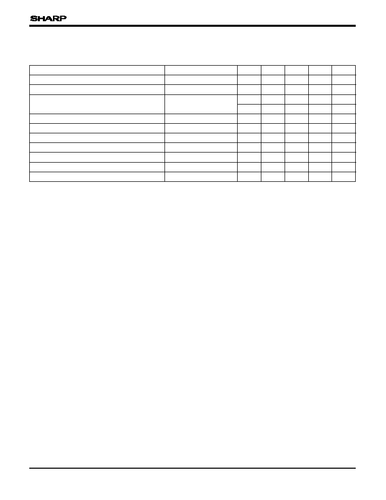
CHARACTERISTICS
(Drive method : 1/30 s frame accumulation)
(T
A
= +25 ∞C, Operating conditions : The typical values specified in "RECOMMENDED OPERATING CONDITIONS".
Color temperature of light source : 3 200 K, IR cut-off filter (CM-500, 1 mmt) is used.)
PARAMETER
SYMBOL
MIN.
TYP.
MAX.
UNIT
NOTE
Standard output voltage
V
O
150
mV
2
Photo response non-uniformity
PRNU
10
%
3
Saturation output voltage
V
SAT
470
550
mV
4
Dark output voltage
V
DARK
0.5
3.0
mV
1, 6
Dark signal non-uniformity
DSNU
0.5
2.0
mV
1, 7
Sensitivity (green channel)
R
140
200
mV
8
Smear ratio
SMR
≠75
≠65
dB
9
Image lag
AI
1.0
%
10
Blooming suppression ratio
ABL
500
11
Output transistor drain current
I
OD
4.0
8.0
mA
NOTES :
∑ Within the recommended operating conditions of V
OD
,
V
OFD
of the internal output satisfies with ABL larger than
500 times exposure of the standard exposure conditions,
and V
SAT
larger than 340 mV.
1. T
A
= +60 ∞C
2. The average output voltage of G signal under uniform
illumination. The standard exposure conditions are
defined as when Vo is 150 mV.
3. The image area is divided into 10 x 10 segments under
the standard exposure conditions. Each segment's
voltage is the average output voltage of all pixels within
the segment. PRNU is defined by (Vmax ≠ Vmin)/Vo,
where Vmax and Vmin are the maximum and minimum
values of each segment's voltage respectively.
4. The image area is divided into 10 x 10 segments. Each
segment's voltage is the average output voltage of all
pixels within the segment. V
SAT
is the minimum
segment's voltage under 10 times exposure of the
standard exposure conditions. The operation of OFDC is
high. (for still image capturing)
5. The image area is divided into 10 x 10 segments. Each
segment's voltage is the average output voltage of all
pixels within the segment. V
SAT
is the minimum
segment's voltage under 10 times exposure of the
standard exposure conditions. The operation of OFDC is
low.
6. The average output voltage under non-exposure
conditions.
7. The image area is divided into 10 x 10 segments under
non-exposure conditions. DSNU is defined by (Vdmax ≠
Vdmin), where Vdmax and Vdmin are the maximum and
minimum values of each segment's voltage respectively.
8. The average output voltage of G signal when a 1 000
lux light source with a 90% reflector is imaged by a lens
of F4, f50 mm.
9. The sensor is exposed only in the central area of V/10
square with a lens at F4, where V is the vertical image
size. SMR is defined by the ratio of the output voltage
detected during the vertical blanking period to the
maximum output voltage in the V/10 square.
10. The sensor is exposed at the exposure level
corresponding to the standard conditions. AI is defined
by the ratio of the output voltage measured at the 1st
field during the non-exposure period to the standard
output voltage.
11. The sensor is exposed only in the central area of V/10
square, where V is the vertical image size. ABL is
defined by the ratio of the exposure at the standard
conditions to the exposure at a point where blooming is
observed.
5
mV
420
340